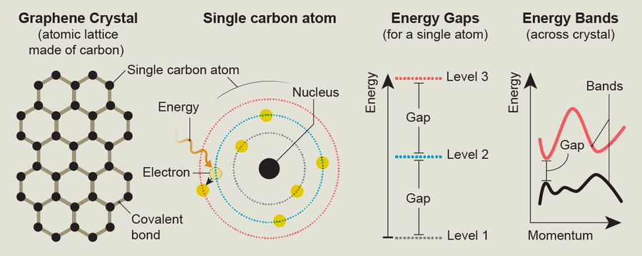
Many seemingly mundane materials, such as the stainless steel on refrigerators or the quartz in a countertop, harbor fascinating physics inside them. These materials are crystals, which in physics means they are made of highly ordered repeating patterns of regularly spaced atoms called atomic lattices. How electrons move through a lattice, hopping from atom to atom, determines many of a solid's properties, such as its color, transparency, and ability to conduct heat and electricity. For example, metals are shiny because they contain lots of free electrons that can absorb light and then reemit most of it, making their surfaces gleam.
In certain crystals the behavior of electrons can create properties that are much more exotic. The way electrons move inside graphene—a crystal made of carbon atoms arranged in a hexagonal lattice—produces an extreme version of a quantum effect called tunneling, whereby particles can plow through energy barriers that classical physics says should block them. Graphene also exhibits a phenomenon called the quantum Hall effect: the amount of electricity it conducts increases in specific steps whose size depends on two fundamental constants of the universe. These kinds of properties make graphene intrinsically interesting as well as potentially useful in applications ranging from better electronics and energy storage to improved biomedical devices.
I and other physicists would like to understand what's going on inside graphene on an atomic level, but it's difficult to observe action at this scale with current technology. Electrons move too fast for us to capture the details we want to see. We've found a clever way to get around this limitation, however, by making matter out of light. In place of the atomic lattice, we use light waves to create what we call an optical lattice. Our optical lattice has the exact same geometry as the atomic lattice. In a recent experiment, for instance, my team and I made an optical version of graphene with the same honeycomb lattice structure as the standard carbon one. In our system, we make cold atoms hop around a lattice of bright and dim light just as electrons hop around the carbon atoms in graphene.
With cold atoms in an optical lattice, we can magnify the system and slow down the hopping process enough to actually see the particles jumping around and make measurements of the process. Our system is not a perfect emulation of graphene, but for understanding the phenomena we're interested in, it's just as good. We can even study lattice physics in ways that are impossible in solid-state crystals. Our experiments revealed special properties of our synthetic material that are directly related to the bizarre physics manifesting in graphene.
Topological Materials
The crystal phenomena we investigate result from the way quantum mechanics limits the motion of wavelike particles. After all, although electrons in a crystal have mass, they are both particles and waves (the same is true for our ultracold atoms). In a solid crystal these limits restrict a single electron on a single atom to only one value of energy for each possible movement pattern (called a quantum state). All other amounts of energy are forbidden. Different states have separate and distinct—discrete—energy values. But a chunk of solid crystal the size of a grape typically contains more atoms (around 1023) than there are grains of sand on Earth. The interactions between these atoms and electrons cause the allowed discrete energy values to spread out and smear into allowed ranges of energy called bands. Visualizing a material's energy band structure can immediately reveal something about that material's properties.
For instance, a plot of the band structure of silicon crystal, a common material used to make rooftop solar cells, shows a forbidden energy range—also known as a band gap—that is 1.1 electron volts wide. If electrons can jump from states with energies below this gap to states with energies above the gap, they can flow through the crystal. Fortunately for humanity, the band gap of this abundant material overlaps well with the wavelengths present in sunlight. As silicon crystal absorbs sunlight, electrons begin to flow through it—allowing solar panels to convert light into usable electricity.
The band structure of certain crystals defines a class of materials known as topological. In mathematics, topology describes how shapes can be transformed without being fundamentally altered. “Transformation” in this context means to deform a shape—to bend or stretch it—without creating or destroying any kind of hole. Topology thus distinguishes baseballs, sesame bagels and shirt buttons based purely on the number of holes in each object.
Topological materials have topological properties hidden in their band structure that similarly allow some kind of transformation while preserving something essential. These topological properties can lead to measurable effects. For instance, some topological materials allow electrons to flow only around their edges and not through their interior. No matter how you deform the material, the current will still flow only along its surface.
I have become particularly interested in certain kinds of topological material: those that are two-dimensional. It may sound odd that 2-D materials exist in our 3-D world. Even a single sheet of standard printer paper, roughly 0.004 inch thick, isn't truly 2-D—its thinnest dimension is still nearly one million atoms thick. Now imagine shaving off most of those atoms until only a single layer of them remains; this layer is a 2-D material. In a 2-D crystal, the atoms and electrons are confined to this plane because moving off it would mean exiting the material entirely.
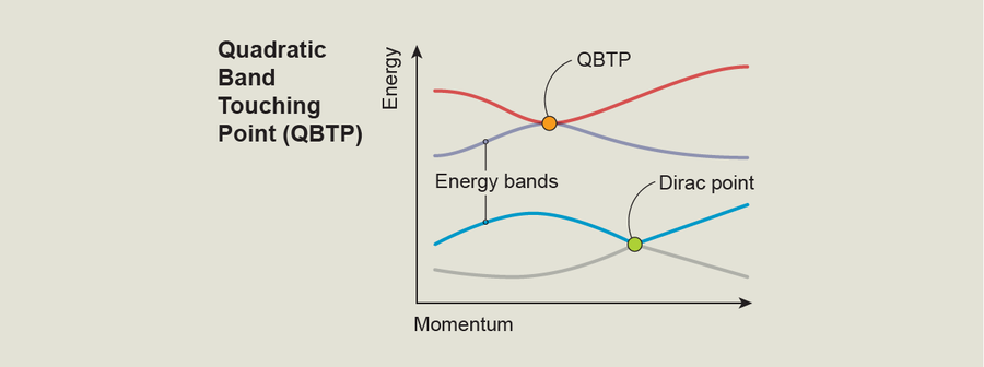
Graphene is an example of a 2-D topological material. To me, the most intriguing thing about graphene is that its band structure contains special spots known as Dirac points. These are positions where two energy bands take on the same value, meaning that at these points electrons can easily jump from one energy band to another. One way to understand Dirac points is to study a plot of the energy of different bands versus an electron's momentum—a property associated with the particle's kinetic energy. Such plots show how an electron's energy changes with its movement, giving us a direct probe into the physics we're interested in. In these plots, a Dirac point looks like a place where two energy bands touch; at this point they're equal, but away from this point the gap between the bands grows linearly. Graphene's Dirac points and the associated topology are connected to this material's ability to display a form of the quantum Hall effect that's unique even among 2-D materials—the half-integer quantum Hall effect—and the special kind of tunneling possible within it.
Artificial Crystals
To understand what's happening to electrons at Dirac points, we need to observe them up close. Our optical lattice experiments are the perfect way to do this. They offer a highly controllable replica of the material that we can uniquely manipulate in a laboratory. As substitutes for the electrons, we use ultracold rubidium atoms chilled to temperatures roughly 10 million times colder than outer space. And to simulate the graphene lattice, we turn to light.
Light is both a particle and a wave, which means light waves can interfere with one another, either amplifying or canceling other waves depending on how they are aligned. We use the interference of laser light to make patterns of bright and dark spots, which become the lattice. Just as electrons in real graphene are attracted to certain positively charged areas of a carbon hexagon, we can arrange our optical lattices so ultracold atoms are attracted to or repelled from analogous spots in them, depending on the wavelength of the laser light that we use. Light with just the right energy (resonant light) landing on an atom can change the state and energy of an electron within it, imparting forces on the atom. We typically use “red-detuned” optical lattices, which means the laser light in the lattice has a wavelength that's longer than the wavelength of the resonant light. The result is that the rubidium atoms feel an attraction to the bright spots arranged in a hexagonal pattern.
We now have the basic ingredients for an artificial crystal. Scientists first imagined these ultracold atoms in optical lattices in the late 1990s and constructed them in the early 2000s. The spacing between the lattice points of these artificial crystals is hundreds of nanometers rather than the fractions of a nanometer that separate atoms in a solid crystal. This larger distance means that artificial crystals are effectively magnified versions of real ones, and the hopping process of atoms within them is much slower, allowing us to directly image the movements of the ultracold atoms. In addition, we can manipulate these atoms in ways that aren't possible with electrons.

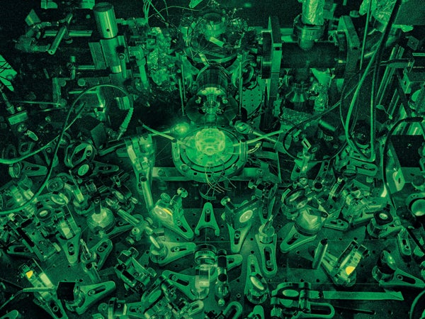
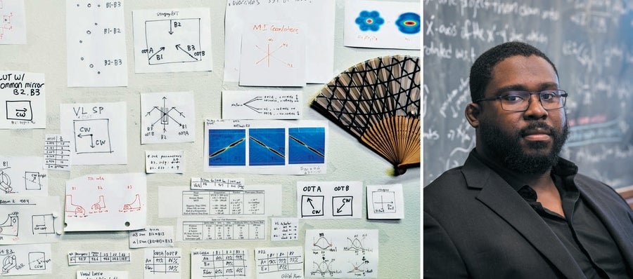
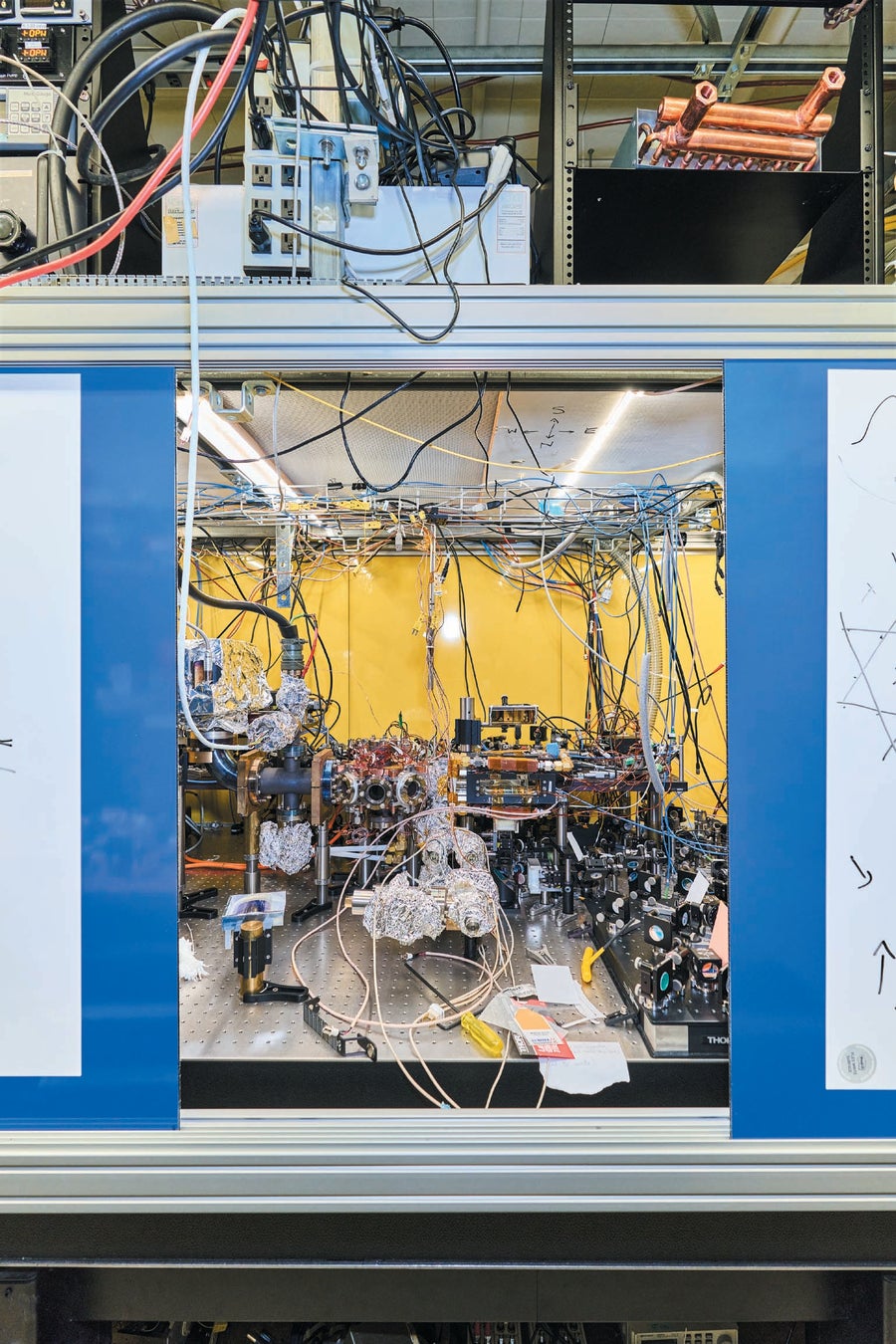
I was a postdoctoral researcher in the Ultracold Atomic Physics group at the University of California, Berkeley, from 2019 to 2022. The lab there has two special tables (roughly one meter wide by two and a half meters long by 0.3 meter high), each weighing roughly one metric ton and floating on pneumatic legs that dampen vibrations. Atop each table lie hundreds of optical components: mirrors, lenses, light detectors, and more. One table is responsible for producing laser light for trapping, cooling and imaging rubidium atoms. The other table holds an “ultrahigh” vacuum chamber made of steel with a vacuum pressure less than that of low-Earth orbit, along with hundreds more optical components.
The vacuum chamber has multiple, sequential compartments with different jobs. In the first compartment, we heat a five-gram chunk of rubidium metal to more than 100 degrees Celsius, which causes it to emit a vapor of rubidium atoms. The vapor gets blasted into the next compartment like water spraying from a hose. In the second compartment, we use magnetic fields and laser light to slow the vapor down. The sluggish vapor then flows into another compartment: a magneto-optical trap, where it is captured by an arrangement of magnetic fields and laser light. Infrared cameras monitor the trapped atoms, which appear on our viewing screen as a bright glowing ball. At this point the atoms are colder than liquid helium.
We then move the cold cloud of rubidium atoms into the final chamber, made entirely of quartz. There we shine both laser light and microwaves on the cloud, which makes the warmest atoms evaporate away. This step causes the rubidium to transition from a normal gas to an exotic phase of matter called a Bose-Einstein condensate (BEC). In a BEC, quantum mechanics allows atoms to delocalize—to spread out and overlap with one another so that all the atoms in the condensate act in unison. The temperature of the atoms in the BEC is less than 100 nanokelvins, one billion times colder than liquid nitrogen.
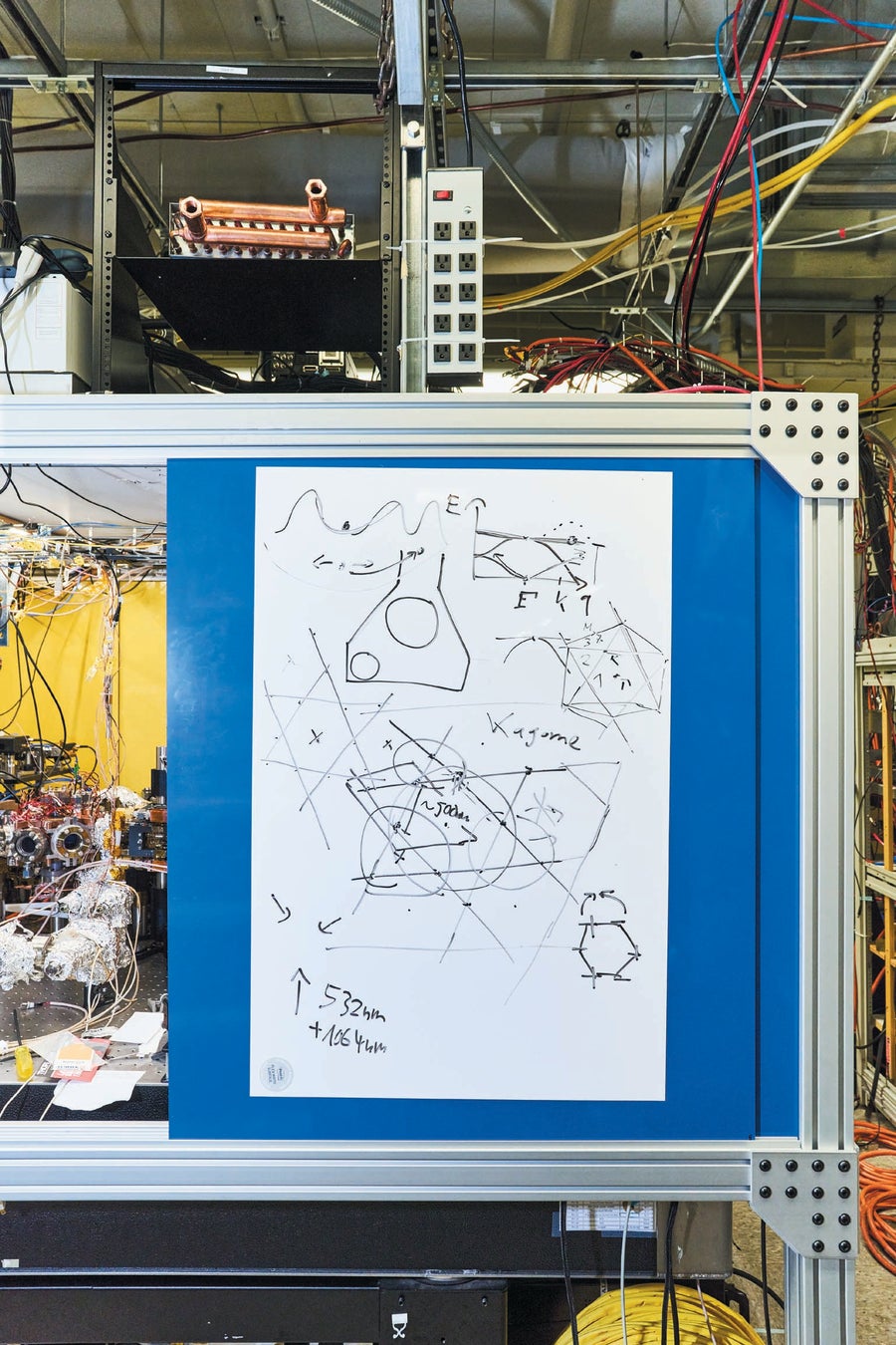
At this point we shine three laser beams separated by 120 degrees into the quartz cell (their shape roughly forms the letter Y). At the intersection of the three beams, the lasers interfere with one another and produce a 2-D optical lattice that looks like a honeycomb pattern of bright and dark spots. We then move the optical lattice so it overlaps with the BEC. The lattice has plenty of space for atoms to hop around, even though it extends over a region only as wide as a human hair. Finally, we collect and analyze pictures of the atoms after the BEC has spent some time in the optical lattice. As complex as it is, we go through this entire process once every 40 seconds or so. Even after years of working on this experiment, when I see it play out, I think to myself, “Wow, this is incredible!”
The Singularity
Like real graphene, our artificial crystal has Dirac points in its band structure. To understand why these points are significant topologically, let's go back to our graph of energy versus momentum, but this time let's view it from above so we see momentum plotted in two directions—right and left, and up and down. Imagine that the quantum state of the BEC in the optical lattice is represented by an upward arrow at position one (P1) and that a short, straight path separates P1 from a Dirac point at position two (P2).
To move our BEC on this graph toward the Dirac point, we need to change its momentum—in other words, we must actually move it in physical space. To put the BEC at the Dirac point, we need to give it the precise momentum values corresponding to that point on the plot. It turns out that it's easier, experimentally, to shift the optical lattice—to change its momentum—and leave the BEC as is; this movement gives us the same end result. From an atom's point of view, a stationary BEC in a moving lattice is the same as a moving BEC in a stationary lattice. So we adjust the position of the lattice, effectively giving our BEC a new momentum and moving it over on our plot.
If we adjust the BEC's momentum so that the arrow representing it moves slowly on a straight path from P1 toward P2 but just misses P2 (meaning the BEC has slightly different momentum than it needs to reach P2), nothing happens—its quantum state is unchanged. If we start over and move the arrow even more slowly from P1 toward P2 on a path whose end is even closer to—but still does not touch—P2, the state again is unchanged.
Now imagine that we move the arrow from P1 directly through P2—that is, we change the BEC's momentum so that it's exactly equal to the value at the Dirac point: we will see the arrow flip completely upside down. This change means the BEC's quantum state has jumped from its ground state to its first excited state.
What if instead we move the arrow from P1 to P2, but when it reaches P2, we force it to make a sharp left or right turn—meaning that when the BEC reaches the Dirac point, we stop giving it momentum in its initial direction and start giving it momentum in a direction perpendicular to the first one? In this case, something special happens. Instead of jumping to an excited state as if it had passed straight through the Dirac point and instead of going back down to the ground state as it would if we had turned it fully around, the BEC ends up in a superposition when it exits the Dirac point at a right angle. This is a purely quantum phenomenon in which the BEC enters a state that is both excited and not. To show the superposition, our arrow in the plot rotates 90 degrees.
Our experiment was the first to move a BEC through a Dirac point and then turn it at different angles. These fascinating outcomes show that these points, which had already seemed special based on graphene's band structure, are truly exceptional. And the fact that the outcome for the BEC depends not just on whether it passes through a Dirac point but on the direction of that movement shows that at the point itself, the BEC's quantum state can't be defined. This shows that the Dirac point is a singularity—a place where physics is uncertain.
We also measured another interesting pattern. If we moved the BEC faster as it traveled near, but not through, the Dirac point, the point would cause a rotation of the BEC's quantum state that made the point seem larger. In other words, it encompassed a broader range of possible momentum values than just the one precise value at the point. The more slowly we moved the BEC, the smaller the Dirac point seemed. This behavior is uniquely quantum mechanical in nature. Quantum physics is a trip!
Although I just described our experiment in a few paragraphs, it took six months of work to get results. We spent lots of time developing new experimental capabilities that had never been used before. We were often unsure whether our experiment would work. We faced broken lasers, an accidental 10-degree-C temperature spike in the lab that misaligned all the optical components (there went three weeks), and disaster when the air in our building caused the lab's temperature to fluctuate, preventing us from creating a BEC. A great deal of persistent effort carried us through and eventually led to our measuring a phenomenon even more exciting than a Dirac point: another kind of singularity.
Geometric Surprises
Before we embarked on our experiment, a related project with artificial crystals in Germany showed what happens when a BEC moves in a circular path around a Dirac point. This team manipulated the BEC's momentum so that it took on values that would plot a circle in the chart of left momentum versus up-down momentum. While going through these transformations, the BEC never touched the Dirac point. Nevertheless, moving around the point in this pattern caused the BEC to acquire something called a geometric phase—a term in the mathematical description of its quantum phase that determines how it evolves. Although there is no physical interpretation of a geometric phase, it's a very unusual property that appears in quantum mechanics. Not every quantum state has a geometric phase, so the fact that the BEC had one here is special. What's even more special is that the phase was exactly π.
My team decided to try a different technique to confirm the German group's measurement. By measuring the rotation of the BEC's quantum state as we turned it away from the Dirac point at different angles, we reproduced the earlier findings. We discovered that the BEC's quantum state “wraps” around the Dirac point exactly once. Another way to say this is that as you move a BEC through momentum space all the way around a Dirac point, it goes from having all its particles in the ground state to having all its particles in the first excited state, and then they all return to the ground state. This measurement agreed with the German study's results.
This wrapping, independent of a particular path or the speed the path is traveled, is a topological property associated with a Dirac point and shows us directly that this point is a singularity with a so-called topological winding number of 1. In other words, the winding number tells us that after a BEC's momentum makes a full circle, it comes back to the state it started in. This winding number also reveals that every time it goes around the Dirac point, its geometric phase increases by π.
Furthermore, we discovered that our artificial crystal has another kind of singularity called a quadratic band touching point (QBTP). This is another point where two energy bands touch, making it easy for electrons to jump from one to another, but in this case it's a connection between the second excited state and the third (rather than the ground state and the first excited state as in a Dirac point). And whereas the gap between energy bands near a Dirac point grows linearly, in a QBTP it grows quadratically.
In real graphene, the interactions between electrons make QBTPs difficult to study. In our system, however, QBTPs became accessible with just one weird trick.
Well, it's not really so weird, nor is it technically a trick, but we did figure out a specific technique to investigate a QBTP. It turns out that if we give the BEC a kick and get it moving before we load it into the optical lattice, we can access a QBTP and study it with the same method we used to investigate the Dirac point. Here, in the plot of momentum space, we can imagine new points P3 and P4, where P3 is an arbitrary starting point in the second excited band and a QBTP lies at P4. Our measurements showed that if we move the BEC from P3 directly through P4 and turn it at various angles, just as we did with the Dirac point, the BEC's quantum state wraps exactly twice around the QBTP. This result means the BEC's quantum state picked up a geometric phase of exactly 2π. Correspondingly, instead of a topological winding number of 1, like a Dirac point has, we found that a QBTP has a topological winding number of 2, meaning that the state must rotate in momentum space around the point exactly twice before it returns to the quantum state it started in.
This measurement was hard-won. We tried nearly daily for an entire month before it eventually worked—we kept finding fluctuations in our experiment whose sources were hard to pinpoint. After much effort and clever thinking, we finally saw the first measurement in which a BEC's quantum state exhibited wrapping around a QBTP. At that moment I thought, “Oh, my goodness, I might actually land a job as a professor.” More seriously, I was excited that our measurement technique showed itself to be uniquely suited to reveal this property of a QBTP singularity.
These singularities, with their strange geometric phases and winding numbers, may sound esoteric. But they are directly related to the tangible properties of the materials we study—in this case the special abilities of graphene and its promising future applications. All these changes that occur in the material's quantum state when it moves through or around these points manifest in cool and unusual phenomena in the real world.
Scientists have predicted, for instance, that QBTPs in solid materials are associated with a type of exotic high-temperature superconductivity, as well as anomalous properties that alter the quantum Hall effect and even electric currents in materials whose flow is typically protected, via topology, from disruption. Before attempting to further investigate this exciting physics, we want to learn more about how interactions between atoms in our artificial crystal change what we observe in our lab measurements.
In real crystals, the electrons interact with one another, and this interaction is usually quite important for the most striking physical effects. Because our experiment was the first of its kind, we took care to ensure that our atoms interacted only minimally to keep things simple. An exciting question we can now pose is: Could interactions cause a QBTP singularity to break apart into multiple Dirac points? Theory suggests this outcome may be possible. We look forward to cranking up the interatomic interaction strength in the lab and seeing what happens.
